
© 2009 Microchip Technology Inc. DS39705B-page 17-1
10-Bit A/D
Converter
17
Section 17. 10-Bit A/D Converter
HIGHLIGHTS
This section of the manual contains the following major topics:
17.1 Introduction ................................................................................................................. 17-2
17.2 A/D Terminology and Conversion Sequence .............................................................. 17-4
17.3 Registers..................................................................................................................... 17-6
17.4 A/D Module Configuration......................................................................................... 17-13
17.5 Initialization ............................................................................................................... 17-16
17.6 Controlling the Sampling Process............................................................................. 17-17
17.7 Controlling the Conversion Process.......................................................................... 17-17
17.8 A/D Results Buffer..................................................................................................... 17-23
17.9 Conversion Sequence Examples.............................................................................. 17-25
17.10 A/D Sampling Requirements..................................................................................... 17-33
17.11 Transfer Function ...................................................................................................... 17-34
17.12 A/D Accuracy/Error ................................................................................................... 17-35
17.13 Operation During Sleep and Idle Modes................................................................... 17-35
17.14 Effects of a Reset...................................................................................................... 17-36
17.15 Register Maps........................................................................................................... 17-37
17.16 Electrical Specifications............................................................................................. 17-38
17.17 Design Tips ............................................................................................................... 17-39
17.18 Related Application Notes......................................................................................... 17-40
17.19 Revision History ........................................................................................................ 17-41

PIC24F Family Reference Manual
DS39705B-page 17-2 © 2009 Microchip Technology Inc.
17.1 INTRODUCTION
The PIC24F 10-bit A/D Converter has the following key features:
• Successive Approximation Register (SAR) Conversion
• Conversion Speeds of up to 500 ksps
• Up to 16 External Analog Input Channels
• Multiple Internal Reference Input Channels (select devices only)
• External Voltage Reference Input Pins
• Unipolar Differential Sample-and-Hold (S/H) Amplifier
• Automatic Channel Scan mode
• Selectable Conversion Trigger Source
• 16-Word Conversion Result Buffer
• Selectable Buffer Fill modes
• Four Options for Results Alignment
• Operation during CPU Sleep and Idle modes
The 10-bit A/D Converter module accepts a single analog signal at any one instant and converts
it to a corresponding 10-bit digital value. It accomodates up to 16 analog inputs and separate ref-
erence inputs; the actual number available on a particular device depends on the package size.
The heart of the module is a Successive Approximation Register (SAR) type of A/D Converter.
Hardware features surrounding the SAR provide flexible configuration and hardware support for
automatic operation, and minimize software overhead, especially in high-speed operation. The
three major sections surrounding the ADC are analog input selection, a memory mapped output
buffer, and timing and control functions.
An internal Sample-and-Hold (S/H) amplifier acquires a sample of an input signal, then holds that
value constant during the conversion process. A combination of input multiplexers selects the
signal to be converted from multiple analog input pins. The whole multiplexer path includes pro-
vision for differential analog input, although the number of negative input pins is limited, and the
signal difference must remain positive (i.e., unipolar). The sampled voltage is held and converted
to a digital value, which strictly speaking, represents the ratio of that input voltage to a reference
voltage. Configuration choices allow connection of an external reference or use of the device
power and ground (AV
DD and AVSS). Reference and input signal pins are assigned differently
depending on the particular device.
An array of timing and control selections allow the user to create flexible scanning sequences.
Conversions can be started individually by program control, continuously free running, or triggered
by selected hardware events. A single channel may be repeatedly converted; alternate conver-
sions may be performed on two channels, or any or all of the channels may be sequentially
scanned and converted according to a user-defined bit map. The resulting conversion output is a
10-bit digital number which can be signed or unsigned, left or right justified.
Conversions are automatically stored in a dedicated 16-word buffer, allowing for multiple succes-
sive readings to be taken before software service is needed. Successive conversions are placed
into sequential buffer locations. Alternatively, the buffer can be split into two 8-word sections for
simultaneous conversion and read operations. The module sets its interrupt flag after a selectable
number of conversions, from one to sixteen, when the whole buffer can be read. After the interrupt,
the sequence restarts at the beginning of the buffer. When the interrupt flag is set according to the
earlier selection, scan selections and the Output Buffer Pointer return to their starting positions.
A simplified block diagram for the module is shown in Figure 17-1.

© 2009 Microchip Technology Inc. DS39705B-page 17-3
Section 17. 10-Bit A/D Converter
10-Bit A/D
Converter
17
Figure 17-1: 10-Bit A/D Converter Block Diagram
Comparator
10-Bit SAR Conversion Logic
VREF+
DAC
AN12
AN13
AN14
AN15
AN8
AN9
AN10
AN11
AN4
AN5
AN6
AN7
AN0
AN1
AN2
AN3
VREF-
Sample Control
S/H
AVSS
AVDD
ADC1BUF0:
ADC1BUFF
AD1CON1
AD1CON2
AD1CON3
AD1CHS
AD1PCFG(L)
AD1PCFGH
(2)
Control Logic
Data Formatting
Input MUX Control
Conversion Control
Pin Config. Control
Internal Data Bus
16
VR+VR-
MUX A
MUX B
VINH
VINL
VINH
VINH
VINL
VINL
VR+
V
R-
VR Select
VBG
(1)
VBG/2
(1)
AD1CSSL
AD1CSSH
(2)
Note 1: Internal analog channels are implemented in select devices only. Different device families implement different
combinations of channels. Refer to the specific device data sheet for details.
2: Implemented in select devices only.
CTMU
(1)
VDDCORE
(1)
AVSS
(1)
AVDD
(1)

PIC24F Family Reference Manual
DS39705B-page 17-4 © 2009 Microchip Technology Inc.
17.2 A/D TERMINOLOGY AND CONVERSION SEQUENCE
Sample time is the time that the A/D module’s S/H amplifier is connected to the analog input pin.
The sample time may be started and ended automatically by the A/D Converter’s hardware or
under direct program control. There is a minimum sample time to ensure that the S/H amplifier
will give sufficient accuracy for the A/D conversion.
Conversion time is the time required for the A/D Converter to convert the voltage held by the
S/H amplifier. The conversion trigger ends the sampling time and begins an A/D conversion or a
repeating sequence. The conversion trigger sources can be taken from a variety of hardware
sources or can be controlled directly in software. An A/D conversion requires one A/D clock cycle
(T
AD) to convert each bit of the result, plus two additional clock cycles, or a total of 12 TAD cycles
for a 10-bit conversion. When the conversion is complete, the result is loaded into one of 16 A/D
result buffers. The S/H can be reconnected to the input pin and a CPU interrupt may be gener-
ated. The sum of the sample time and the A/D conversion time provides the total A/D sequence
time. Figure 17-2 shows the basic conversion sequence and the relationship between intervals.
The conversion trigger sources can be taken from a variety of hardware sources, or can be
controlled directly by software. One of the conversion trigger options is an auto-conversion,
which uses a counter and the A/D clock to set the time between auto-conversions. The
Auto-Sample mode and auto-conversion trigger can be used together to provide continuous
automatic conversions without software intervention.
Figure 17-2: A/D Sample/Convert Sequence
Sample Time
A/D Conversion Time
Total A/D Sequence Time
S/H amplifier is connected to
the analog input pin for sampling.
Input disconnected; S/H amplifier holds signal.
Conversion trigger starts A/D conversion.
Conversion complete, result is loaded
into A/D Buffer register.
Interrupt is generated (optional).
© 2009 Microchip Technology Inc. DS39705B-page 17-5
Section 17. 10-Bit A/D Converter
10-Bit A/D
Converter
17
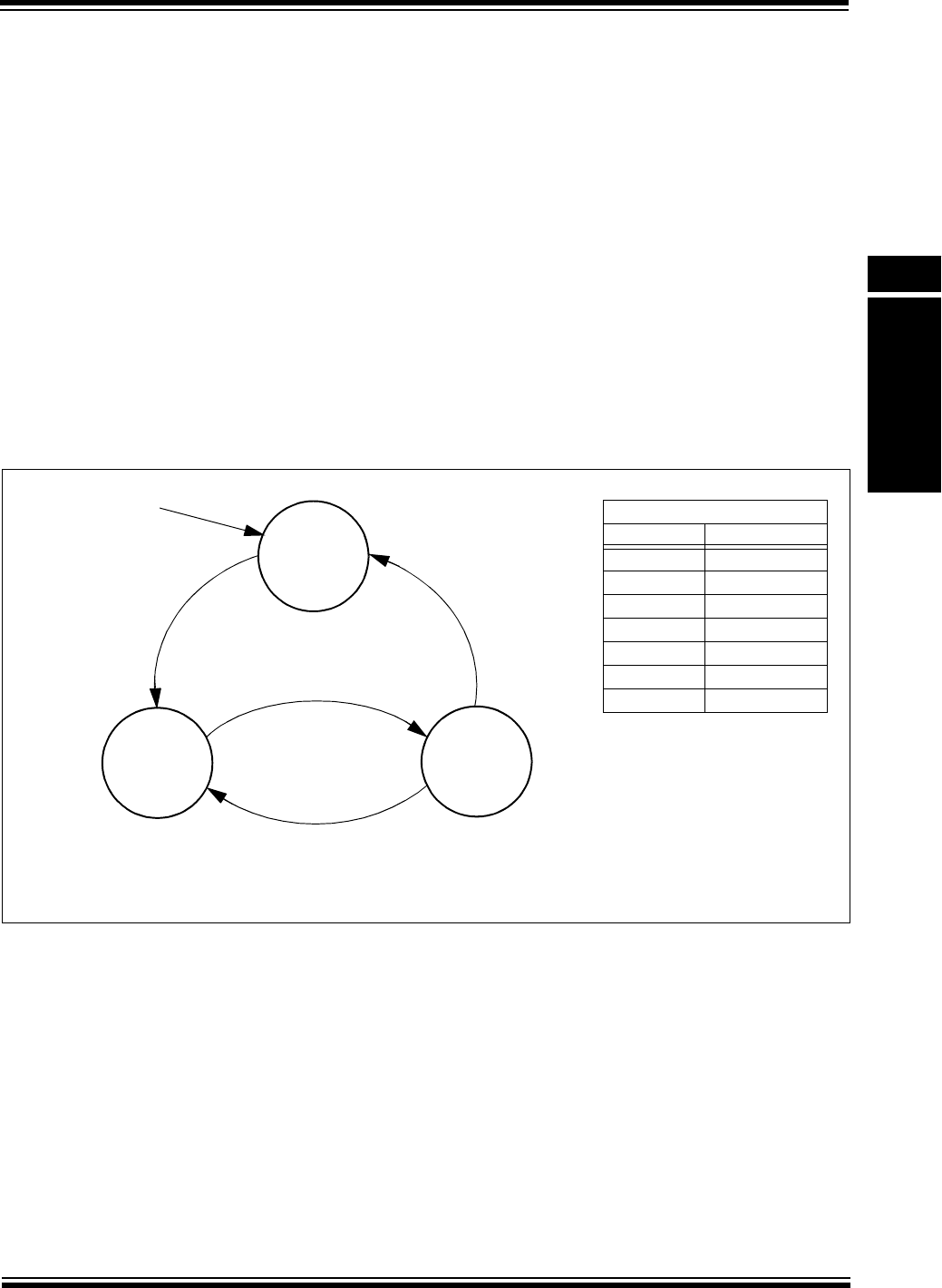
17.2.1 Operation as a State Machine
The A/D conversion process can be thought of in terms of a finite state machine (Figure 17-3).
The sample state represents the time that the input channel is connected to the S/H amplifier and
the signal is passed to the converter input. The convert state is transitory; the module enters this
state as soon as it exits the sample state and transitions to a different state when that is done.
The inactive state is the default state prior to module initialization and following a
software-controlled conversion; it can be avoided in operation by using Auto-Sample mode.
Machine states are identified by the state of several control and status bits in AD1CON1
(Register 17-1).
If the module is configured for Auto-Sample mode, the operation “ping-pongs” continuously
between the sample and convert states. The module automatically selects the input channels to
be sampled (if channel scanning is enabled), while the selected conversion trigger source paces
the entire operation. Any time that Auto-Sample mode is not used for conversion, it is available
for the sample state.The user needs to make certain that acquisition time is sufficient, in addition
to accounting for the normal concerns about system throughput.
Whenever the issue of sampling time is important, the significant event is the transition from
sample to convert state. This is the point where the Sample-and-Hold aperture closes and it is
essentially the signal value at this instant which is applied to the A/D for conversion to digital.
Figure 17-3: A/D Module State Machine Model
INACTIVE
SAMPLE
CONVERT
SAMP = 0
DONE = 1
SAMP = 0
DONE =
0
SAMP = 1
DONE = x
SAMP 0
→1
ASAM = 1 and DONE 0→1
ASAM = 0
and
SSRC Trigger Events (see table)
DONE 0
→1
SSRC Trigger Events
SSRC<2:0> Event
0 SAMP 1
→0
1INT0
2Timer3
3* Timer5
4* CTMU
6* Alt. CTMU
7Auto
* Available in select devices only.
Device Reset
Legend: HW = automatic hardware event; SW = software controlled event.
Note: See Register 17-1 for definitions of the ASAM, SAMP, DONE and SSRC<2:0> bits.
SW
HW
HW
ASAM 0
→1 or

PIC24F Family Reference Manual
DS39705B-page 17-6 © 2009 Microchip Technology Inc.
17.3 REGISTERS
The 10-bit A/D Converter module uses a total of 22 registers for its operation. All registers are
mapped in the data memory space.
17.3.1 Control Registers
Depending on the specific device, the module has up to eight control and status registers:
• AD1CON1: A/D Control Register 1
• AD1CON2: A/D Control Register 2
• AD1CON3: A/D Control Register 3
• AD1CHS: A/D Input Channel Select Register
• AD1PCFG(L) and AD1PCFGH: A/D Port Configuration Registers
• AD1CSSL and AD1CSSH: A/D Input Scan Select Registers
The AD1CON1, AD1CON2 and AD1CON3 registers (Register 17-1, Register 17-2 and
Register 17-3) control the overall operation of the A/D module. This includes enabling the
module, configuring the conversion clock and voltage reference sources, selecting the sampling
and conversion triggers, and manually controlling the sample/convert sequences.
The AD1CHS register (Register 17-4) selects the input channels to be connected to the S/H
amplifier. It also allows the choice of input multiplexers and the selection of a reference source
for differential sampling.
The AD1PCFG (AD1PCFGL in select devices) register (Register 17-5) configures I/O pins as
analog inputs or digital I/Os. For PIC24F devices with the internal reference channels, the
PFCG<17:16> bits in the AD1PCFGH register (Register 17-6) enable these channels for
inclusion in sequential scanning.
The AD1CSSL register (Register 17-7) selects the channels to be included for sequential
scanning. For PIC24F devices with the internal reference channels, the AD1CSSH register
(Register 17-8) selects these channels for inclusion in sequential scanning.
17.3.2 A/D Result Buffers
The module incorporates a 16-word, dual port RAM, called ADC1BUF, to store the A/D results.
Each of the locations is mapped into the data memory space and is separately addressable. The
16 buffer locations are referred to as ADC1BUF0 through ADC1BUFF. The A/D result buffers are
read-only.

© 2009 Microchip Technology Inc. DS39705B-page 17-7
Section 17. 10-Bit A/D Converter
10-Bit A/D
Converter
17
Register 17-1: AD1CON1: A/D Control Register 1
R/W-0 U-0 R/W-0 U-0 U-0 U-0 R/W-0 R/W-0
ADON
—ADSIDL— — —FORM1FORM0
bit 15 bit 8
R/W-0 R/W-0 R/W-0 U-0 U-0 R/W-0 R/W-0, HCS R/C-0, HCS
SSRC2 SSRC1 SSRC0 — — ASAM SAMP DONE
bit 7 bit 0
Legend: C = Clearable bit U = Unimplemented bit, read as ‘0’
R = Readable bit W = Writable bit HCS = Hardware Clearable/Settable bit
-n = Value at POR ‘1’ = Bit is set ‘0’ = Bit is cleared x = Bit is unknown
bit 15 ADON: A/D Operating Mode bit
1 = A/D Converter module is operating
0 = A/D Converter is disabled
bit 14 Unimplemented: Read as ‘0’
bit 13 ADSIDL: Stop in Idle Mode bit
1 = Discontinue module operation when device enters Idle mode
0 = Continue module operation in Idle mode
bit 12-10 Unimplemented: Read as ‘0’
bit 9-8 FORM<1:0>: Data Output Format bits
11 = Signed fractional (sddd dddd dd00 0000)
10 = Fractional (dddd dddd dd00 0000)
01 = Signed integer (ssss sssd dddd dddd)
00 = Integer (0000 00dd dddd dddd)
bit 7-5 SSRC<2:0>: Conversion Trigger Source Select bits (event ends sampling and starts conversion)
111 = Internal counter (auto-convert)
110 = CTMU event (when not implemented as ‘100’)
(1)
101 = Reserved
100 = CTMU event
(1)
011 = Timer5 compare match
(1,2)
010 = Timer3 compare match
(2)
001 = Active transition on INT0 pin (basic sync convert)
000 = Clearing SAMP bit (full program control)
bit 4-3 Unimplemented: Read as ‘0’
bit 2 ASAM: A/D Sample Auto-Start Mode bit
1 = Sampling begins immediately after last conversion completes; SAMP bit is automatically set
0 = Sampling begins when SAMP bit is set
bit 1 SAMP: A/D Sample Enable Mode Mode bit
1 = A/D Sample-and-Hold amplifier is sampling
0 = A/D Sample-and-Hold amplifier is holding
When ASAM = 0, writing ‘1’ to this bit starts sampling. When SSRC<2:0> = 000, writing ‘0’ to this bit
will end sampling and start conversion.
bit 0 DONE: A/D Conversion Status bit
1 = A/D conversion is done
0 = A/D conversion is not done or has not started
Clearing this bit will not affect any operation in progress; it is cleared by software or start of a new conversion.
Note 1: This option is available in select devices only. Refer to the specific device data sheet.
2: Use Timer3 or Timer5 as a clock divider for a fixed sample rate. The T3CK or T5CK input may also be
selected with this mode to synchronize with an external event by configuring the counter to clock from the
T3CK pin while preset for one pulse. See Section 14. “Timers” for more information.

PIC24F Family Reference Manual
DS39705B-page 17-8 © 2009 Microchip Technology Inc.
Register 17-2: AD1CON2: A/D Control Register 2
R/W-0 R/W-0 R/W-0 r-0 U-0 R/W-0 U-0 U-0
VCFG2 VCFG1 VCFG0
r — CSCNA — —
bit 15 bit 8
R-0 U-0 R/W-0 R/W-0 R/W-0 R/W-0 R/W-0 R/W-0
BUFS
(1)
— SMPI3 SMPI2 SMPI1 SMPI0 BUFM ALTS
bit 7 bit 0
Legend: r = Reserved bit
R = Readable bit W = Writable bit U = Unimplemented bit, read as ‘0’
-n = Value at POR ‘1’ = Bit is set ‘0’ = Bit is cleared x = Bit is unknown
bit 15-13 VCFG<2:0>: Voltage Reference Configuration bits
bit 12 Reserved: Maintain as ‘0’
bit 11 Unimplemented: Read as ‘0’
bit 10 CSCNA: MUX A Channel Scan/Input Channel Select bit
1 = Scan inputs selected by the AD1CSSL register as the MUX A input
0 = Use the channel selected by the CH0SA bits as the MUX A input
bit 9-8 Unimplemented: Read as ‘0’
bit 7 BUFS: Buffer Fill Status bit
(1)
1 = A/D is currently filling ADC1BUF8-ADC1BUFF, user should access data in ADC1BUF0-ADC1BUF7
0 = A/D is currently filling ADC1BUF0-ADC1BUF7, user should access data in ADC1BUF8-ADC1BUFF
bit 6 Unimplemented: Read as ‘0’
bit 5-2 SMPI<3:0>: Sample/Convert Sequences Per Interrupt Selection bits
1111 = Interrupts at the completion of conversion for each 16th sample/convert sequence
1110 = Interrupts at the completion of conversion for each 15th sample/convert sequence
.....
0001 = Interrupts at the completion of conversion for each 2nd sample/convert sequence
0000 = Interrupts at the completion of conversion for each sample/convert sequence
bit 1 BUFM: Buffer Mode Select bit
1 = Buffer configured as two 8-word buffers (ADC1BUF0 to ADC1BUF7 and ADC1BUF8 to
ADC1BUFF)
0 = Buffer configured as one 16-word buffer (ADC1BUF0 to ADC1BUFF)
bit 0 ALTS: Alternate Input Sample Mode Select bit
1 = Alternate between MUX A and MUX B input multiplexer settings on successive conversions,
starting with MUX A
0 = Always uses MUX A input multiplexer settings
Note 1: Only valid when ADC1BUF is functioning as two buffers (BUFM = 1).
VCFG<2:0> VR+VR-
000 AV
DD AVSS
001 External VREF+ Pin AVSS
010 AVDD External VREF- Pin
011 External VREF+ Pin External VREF- Pin
1xx AVDD AVSS

© 2009 Microchip Technology Inc. DS39705B-page 17-9
Section 17. 10-Bit A/D Converter
10-Bit A/D
Converter
17
Register 17-3: AD1CON3: A/D Control Register 3
R/W-0 U-0 U-0 R/W-0 R/W-0 R/W-0 R/W-0 R/W-0
ADRC
— — SAMC4 SAMC3 SAMC2 SAMC1 SAMC0
bit 15 bit 8
R/W-0 R/W-0 R/W-0 R/W-0 R/W-0 R/W-0 R/W-0 R/W-0
ADCS7 ADCS6 ADCS5 ADCS4 ADCS3 ADCS2 ADCS1 ADCS0
bit 7 bit 0
Legend:
R = Readable bit W = Writable bit U = Unimplemented bit, read as ‘0’
-n = Value at POR ‘1’ = Bit is set ‘0’ = Bit is cleared x = Bit is unknown
bit 15 ADRC: A/D Conversion Clock Source bit
1 = A/D internal RC clock
0 = Clock derived from system clock
bit 14-13 Unimplemented: Read as ‘0’
bit 12-8 SAMC<4:0>: Auto-Sample Time bits
11111 = 31 T
AD
·····
00001 = 1 T
AD
00000 = 0 TAD (not recommended)
bit 7-0 ADCS<7:0>: A/D Conversion Clock Period Select bits
(1)
11111111
······ = Reserved
01000000
00111111 = 64 • Tcy
······
00000001 = 2 • T
CY
00000000 = TCY
Note 1: Only valid when using the system clock as the conversion clock (ADRC = 0).

PIC24F Family Reference Manual
DS39705B-page 17-10 © 2009 Microchip Technology Inc.
Register 17-4: AD1CHS: A/D Input Channel Select Register
R/W-0 U-0 U-0
R/W-0
R/W-0 R/W-0 R/W-0 R/W-0
CH0NB
— — CH0SB4
(1)
CH0SB3 CH0SB2 CH0SB1 CH0SB0
bit 15 bit 8
R/W-0 U-0 U-0
R/W-0
R/W-0 R/W-0 R/W-0 R/W-0
CH0NA
— — CH0SA4
(1)
CH0SA3 CH0SA2 CH0SA1 CH0SA0
bit 7 bit 0
Legend:
R = Readable bit W = Writable bit U = Unimplemented bit, read as ‘0’
-n = Value at POR ‘1’ = Bit is set ‘0’ = Bit is cleared x = Bit is unknown
bit 15 CH0NB: S/H Amplifier Negative Input Select for MUX B Multiplexer Setting bit
1 = Negative input is AN1
0 = Negative input is V
R-
bit 14-13 Unimplemented: Read as ‘0’
bit 12-8 CH0SB<4:0>: S/H Amplifier Positive Input Select for MUX B Multiplexer Setting bits
(1)
The number of implemented analog inputs and the bit combinations assigned to them vary significantly
between device families. In general, external analog inputs, AN0 through AN15 (where implemented),
are sequentially assigned from ‘00000’ as shown below. If a sequential input is unimplemented, its
corresponding bit value is also unimplemented.
In addition, some devices implement inputs for internal band gap references, external voltage
references, and other analog modules, such as the CTMU. Refer to the specific device data sheet for
a complete listing of implemented inputs for a particular device.
Any bit combinations not explicitly listed are unimplemented. Using an unimplemented channel for a
conversion will produce unpredictable results.
01111 = Positive input is AN15
01110 = Positive input is AN14
01101 = Positive input is AN13
01100 = Positive input is AN12
01011 = Positive input is AN11
01010 = Positive input is AN10
01001 = Positive input is AN9
01000 = Positive input is AN8
00111 = Positive input is AN7
00110 = Positive input is AN6
00101 = Positive input is AN5
00100 = Positive input is AN4
00011 = Positive input is AN3
00010 = Positive input is AN2
00001 = Positive input is AN1
00000 = Positive input is AN0
bit 7 CH0NA: S/H Amplifier Negative Input Select for MUX A Multiplexer Setting bit
1 = Negative input is AN1
0 = Negative input is V
R-
bit 6-5 Unimplemented: Read as ‘0’
bit 4-0 CH0SA<4:0>: S/H Amplifier Positive Input Select for MUX A Multiplexer Setting bits
(1)
Implemented combinations are identical to those for CH0SB<4:0>.
Note 1: CH0SB4 and CH0SA4 are implemented in select devices only. Their implementation generally indicates
an extended range of input sources from voltage references and other analog modules.

© 2009 Microchip Technology Inc. DS39705B-page 17-11
Section 17. 10-Bit A/D Converter
10-Bit A/D
Converter
17
Register 17-5: AD1PCFG(L): A/D Port Configuration Low Register
(1)
R/W-0 R/W-0 R/W-0 R/W-0 R/W-0 R/W-0 R/W-0 R/W-0
PCFG15 PCFG14 PCFG13 PCFG12 PCFG11 PCFG10 PCFG9 PCFG8
bit 15 bit 8
R/W-0 R/W-0 R/W-0 R/W-0 R/W-0 R/W-0 R/W-0 R/W-0
PCFG7 PCFG6 PCFG5 PCFG4 PCFG3 PCFG2 PCFG1 PCFG0
bit 7 bit 0
Legend:
R = Readable bit W = Writable bit U = Unimplemented bit, read as ‘0’
-n = Value at POR ‘1’ = Bit is set ‘0’ = Bit is cleared x = Bit is unknown
bit 15-0 PCFG<15:0>: Analog Input Pin Configuration Control bits
1 = Pin for corresponding analog channel is in Digital mode; port read input enabled, A/D input
multiplexer input connected to AV
SS
0 = Pin for corresponding analog channel is in Analog mode; port read input disabled, A/D module
samples pin voltage
Note 1: In devices without the internal band gap reference options, this register is named AD1PCFG. In devices
with the band gap options, it is named AD1PCFGL.
Register 17-6: AD1PCFGH: A/D Port Configuration High Register
(1)
U-0 U-0 U-0 U-0 U-0 U-0 U-0 U-0
— — — — — — — —
bit 15 bit 8
U-0 U-0 U-0 U-0 U-0 U-0 R/W-0 R/W-0
— — — — — — PCFG17 PCFG16
bit 7 bit 0
Legend:
R = Readable bit W = Writable bit U = Unimplemented bit, read as ‘0’
-n = Value at POR ‘1’ = Bit is set ‘0’ = Bit is cleared x = Bit is unknown
bit 15-2 Unimplemented: Read as ‘0’
bit 1 PCFG17: A/D Input Band Gap Scan Enable bit
1 = Analog channel disabled from input scan
0 = Internal band gap (V
BG) channel enabled for A/D MUX input
bit 0 PCFG16: A/D Input Half Band Gap Scan Enable bit
1 = Analog channel disabled from input scan
0 = Internal V
BG/2 channel enabled for A/D MUX input
Note 1: AD1PCFGH is implemented in select devices only.

PIC24F Family Reference Manual
DS39705B-page 17-12 © 2009 Microchip Technology Inc.
Register 17-7: AD1CSSL: A/D Input Scan Select Low Register for MUX A
(1)
R/W-0 R/W-0 R/W-0 R/W-0 R/W-0 R/W-0 R/W-0 R/W-0
CSSL15 CSSL14 CSSL13 CSSL12 CSSL11 CSSL10 CSSL9 CSSL8
bit 15 bit 8
R/W-0 R/W-0 R/W-0 R/W-0 R/W-0 R/W-0 R/W-0 R/W-0
CSSL7 CSSL6 CSSL5 CSSL4 CSSL3 CSSL2 CSSL1 CSSL0
bit 7 bit 0
Legend:
R = Readable bit W = Writable bit U = Unimplemented bit, read as ‘0’
-n = Value at POR ‘1’ = Bit is set ‘0’ = Bit is cleared x = Bit is unknown
bit 15-0 CSSL<15:0>: A/D Input Channel Scan Selection bits
1 = Corresponding analog channel, ANx, is selected for sequential scanning on MUX A
0 = Corresponding analog channel is ignored in sequential scanning
Note 1: Only MUX A supports scanning of input channels.
Register 17-8: AD1CSSH: A/D Input Scan Select High Register for MUX A
(1,2)
U-0 U-0 U-0 U-0 U-0 U-0 U-0 U-0
— — — — — — — —
bit 15 bit 8
U-0 U-0 U-0 U-0 U-0 U-0 R/W-0 R/W-0
— — — — — — CSSL17 CSSL16
bit 7 bit 0
Legend:
R = Readable bit W = Writable bit U = Unimplemented bit, read as ‘0’
-n = Value at POR ‘1’ = Bit is set ‘0’ = Bit is cleared x = Bit is unknown
bit 15-2 Unimplemented: Read as ‘0’
bit 1 CSSL17: A/D Input Band Gap Scan Selection bit
1 = Internal band gap (V
BG) channel is selected for sequential scanning on MUX A
0 = Analog channel is ignored in sequential scanning
bit 0 CSSL16: A/D Input Half Band Gap Scan Selection bit
1 = Internal V
BG/2 channel is selected for sequential scanning on MUX A
0 = Analog channel is ignored in sequential scanning
Note 1: Only MUX A supports scanning of input channels.
2: AD1CSSH is implemented in select devices only.

© 2009 Microchip Technology Inc. DS39705B-page 17-13
Section 17. 10-Bit A/D Converter
10-Bit A/D
Converter
17
17.4 A/D MODULE CONFIGURATION
All of the registers described in the previous section must be configured for module operation to
be fully defined. An effective approach is first to describe the signals and sequences for the par-
ticular application. Typically, it is an iterative process to assign signals to port pins, to establish
timing methods and to organize a scanning scheme, as well as to integrate the whole process
with the software design.
The various configuration and control functions of the module are distributed throughout the
module’s six (or eight) control registers. Control functions can be broadly sorted into four groups:
input, timing, conversion and output. Table 17-1 shows the register location of control or status
bits by register.
Table 17-1: A/D Module Fuctions by Registers and Bits
The following steps should be followed for performing an A/D conversion.
1. Configure the A/D module:
• Select voltage reference source to match expected range on analog inputs
• Select the analog conversion clock to match desired data rate with processor clock
• Determine how sampling will occur
• Set the multiplexer input assignments
• Select the desired sample/conversion sequence
• Select the output data format
• Select the number of readings per interrupt
2. Configure A/D interrupt (if required):
• Clear AD1IF bit
• Select A/D interrupt priority
3. Turn on A/D module.
The options for each configuration step are described in the subsequent sections.
17.4.1 Selecting the Voltage Reference Source
The voltage references for A/D conversions are selected using the VCFG<2:0> control bits
(AD1CON2<15:13>). The upper voltage reference (V
R+) and the lower voltage reference (VR-)
may be the internal AV
DD and AVSS voltage rails or the VREF+ and VREF- input pins.
The external voltage reference pins may be shared with the AN0 and AN1 inputs on low pin count
devices. The A/D Converter can still perform conversions on these pins when they are shared
with the V
REF+ and VREF- input pins.
The voltages applied to the external reference pins must meet certain specifications. Refer to
Section 17.16 “Electrical Specifications” for further details.
A/D Function Register(s) Specific Bits
Input AD1CON2 VCFG<2:0>, CSCNA, ALTS
AD1CHS CH0NB, CH0SB<4:0>, CH0NA, CH0SA<4:0>
AD1PCFG(H/L) PCFG<17:16>
(1)
, PCFG<15:0>
AD1CSS(H/L) CSSL<17:16>
(1)
, CSSL<15:0>
Conversion AD1CON1 ADON, ADSIDL, SSRC<2:0>, ASAM, SAMP, DONE
AD1CON2 SMPI<3:0>
Timing AD1CON3 ADRC, SAMC<4:0>, ADCS<7:0>
Output AD1CON1 FORM<1:0>
AD1CON2 BUFS, BUFM
Note 1: Implemented in select devices only.
Note: Do not write to the SSRC, ASAM, BUFS SMPI, BUFM and ALTS bits, or the
AD1CON3 and AD1CSSL registers, while ADON = 1; otherwise, indeterminate
conversion data may result.

PIC24F Family Reference Manual
DS39705B-page 17-14 © 2009 Microchip Technology Inc.
17.4.2 Selecting the A/D Conversion Clock
The A/D Converter has a maximum rate at which conversions may be completed. An analog
module clock, T
AD, controls the conversion timing. The A/D conversion requires 12 clock periods
(12 T
AD). The A/D clock is derived from the device instruction clock.
The period of the A/D conversion clock is software selected using a 6-bit counter. There are
64 possible options for TAD, specified by the ADCS bits in the AD1CON3 register. Equation 17-1
gives the T
AD value as a function of the ADCS control bits and the device instruction cycle clock
period, T
CY. For correct A/D conversions, the A/D conversion clock (TAD) must be selected to
ensure a minimum T
AD time of 75 ns.
Equation 17-1: A/D Conversion Clock Period
The A/D Converter also has its own dedicated RC clock source that can be used to perform
conversions. The A/D RC clock source should be used when conversions are performed while
the device is in Sleep mode. The RC oscillator is selected by setting the ADRC bit
(AD1CON3<15>). When the ADRC bit is set, the ADCS bits have no effect on A/D operation.
17.4.3 Configuring Analog Port Pins
The AD1PCFG register (AD1PCFGL and AD1PCFGH registers in select devices) specifies the
input condition of device pins used as analog inputs. A pin is configured as an analog input when
the corresponding PCFGx bit (AD1PCFG<x>) is cleared. The register is cleared on device
Resets, causing the A/D input pins to be configured for analog inputs by default. When
configured for analog inputs, the associated port I/O digital input buffer is disabled, so it does not
consume current.
For external analog inputs, both the AD1PCFG(L) register and the corresponding TRIS register
bits control the operation of the A/D port pins. The port pins that will function as analog inputs
must also have their corresponding TRIS bits set, specifying the pins as inputs. After a device
Reset, all TRIS bits are set.
If the I/O pin associated with an A/D channel is configured as a digital output (TRIS bit is cleared),
while the pin is configured for Analog mode (AD1PCFG<x> = 0), the port digital output level (V
OH
or VOL) will be converted.
A pin is configured as digital I/O when the corresponding PCFGx bit is set. In this configuration,
the input to the analog multiplexer is connected to AV
SS.
17.4.4 Input Channel Selection
The A/D Converter incorporates two independent sets of input multiplexers (MUX A and MUX B)
that allow users to choose which analog channels are to be sampled. The inputs specified by the
CH0SA bits and CH0NA are collectively called the MUX A inputs. The inputs specified by the
CH0SB bits and CH0NB are collectively called the MUX B inputs.
Note 1: When reading a PORT register, any pin configured as an analog input reads as ‘0’.
2: Analog levels on any pin that is defined as a digital input (including the AN<15:0>
pins) may cause the input buffer to consume current that is out of the device’s
specification.
TCY (ADCS + 1)
ADCS =
– 1
T
AD
TCY
Note: Based on TCY = 2/FOSC, Doze mode and PLL are disabled.
T
AD =

© 2009 Microchip Technology Inc. DS39705B-page 17-15
Section 17. 10-Bit A/D Converter
10-Bit A/D
Converter
17
Functionally, MUX A and MUX B are very similar to each other. Both multiplexers allow any of
the analog input channels to be selected for individual sampling and allow selection of a negative
reference source for differential signals. In addition, MUX A can be configured for sequential
analog channel scanning. This is discussed in more detail in Section 17.4.4.1 “Configuring
MUX A and MUX B Inputs” and Section 17.4.4.3 “Scanning Through Several Inputs”..
17.4.4.1 CONFIGURING MUX A AND MUX B INPUTS
The user may select any one of up to 16 analog inputs to connect to the positive input of the S/H
amplifer. For MUX A, the CH0SA<3:0> bits (AD1CHS<3:0>) normally select the analog channel
for the positive input. For MUX B, the positive channel is selected by the CH0SB<3:0> bits
(AD1CHS<11:8>).
On certain PIC24F devices, users may also select the microcontroller’s internal band gap voltage
reference (V
BG) or one-half of the reference (VBG/2) as the positive input to the S/H amplifier. For
these devices, the CH0SA<4:0> bits (AD1CHS<4:0>) and CH0SB<4:0> bits (AD1CHS<12:8>)
select the positive input.
For the negative (inverting) input of the amplifier, the user has two options, selected by the
CH0NA and CH0NB bits (AD1CHS<7,15>, respectively). Setting either bit selects AN1 as the
multiplexer’s negative input; clearing the bit selects the current V
R- source designated by the
VCFG<2:0> bits (AD1CON2<15:13>).
17.4.4.2 ALTERNATING MUX A AND MUX B INPUT SELECTIONS
By default, the A/D Converter only samples and converts the inputs selected by MUX A. The
ALTS bit (AD1CON2<0>) enables the module to alternate between two sets of inputs selected
by MUX A and MUX B during successive samples.
If the ALTS bit is ‘0’, only the inputs specified by the CH0SA and CH0NA bits are selected for
sampling. When the ALTS bit is ‘1’, the module will alternate between the MUX A inputs on one
sample and the MUX B inputs on the subsequent sample.
If the ALTS bit is ‘1’ on the first sample/convert sequence, the inputs specified by the CH0SA bits
and CH0NA are selected for sampling. On the next sample/convert sequence, the inputs
specified by the CH0SB bits and CH0NB are selected for sampling. This pattern repeats for
subsequent sample conversion sequences.
17.4.4.3 SCANNING THROUGH SEVERAL INPUTS
When using MUX A to select analog inputs, the A/D module has the ability to scan multiple
analog channels. When the CSCNA bit (AD1CON2<10>) is set, the CH0SA bits are ignored and
the channels specified by the AD1CSSL register are sequentially sampled.
Each bit in the AD1CSSL register and AD1CSSH register (when implemented) corresponds to
one of the analog channels. If a bit in the AD1CSSL or AD1CSSH register is set, the correspond-
ing analog channel is included in the scan sequence. Inputs are always scanned from lower to
higher numbered inputs, starting at the first selected channel after each interrupt occurs.
The AD1CSSL or AD1CSSH bits only specify the positive input of the channel. The CH0NA bit
still selects the negative input of the channel during scanning.
Scanning is only available on the MUX A input selection. The MUX B input selection, as specified
by the CH0SB bits, will still select the alternating input. When alternated sampling between
MUX A and MUX B is selected (ALTS = 1), the input will alternate between a set of scanning
inputs specified by the AD1CSSL register and a fixed input specified by the CH0SB bits.
Note: Different PIC24F devices will have different numbers of analog inputs. Verify the
analog input availability against the particular device’s data sheet.
Note: If the number of scanned inputs selected is greater than the number of samples
taken per interrupt, the higher numbered inputs will not be sampled.

PIC24F Family Reference Manual
DS39705B-page 17-16 © 2009 Microchip Technology Inc.
17.4.5 Enabling the Module
When the ADON bit (AD1CON1<15>) is set, the module is fully powered and functional. When
ADON is ‘0’, the module is disabled. The digital and analog portions of the circuit are turned off
for maximum current savings. As the ADC1BUF registers are also part of the A/D module,
clearing ADON may also result in a loss of conversion data.
When enabling the module by setting the ADON bit, the user must wait for the analog stages to
stabilize. For the stabilization time, refer to Section 17.16 “Electrical Specifications”.
17.5 INITIALIZATION
Example 17-1 shows a simple initialization code example for the A/D module. In this particular
configuration, all 16 analog input pins are set up as analog inputs. Operation in Idle mode is
disabled, output data is in unsigned fractional format, and AVDD and AVSS are used for VR+ and
V
R-. The start of sampling, as well as the start of conversion (conversion trigger), are performed
directly in software. Scanning of inputs is disabled and an interrupt occurs after every
sample/convert sequence (1 conversion result) with only one channel (AN0) being converted. The
A/D conversion clock is T
CY/2.
This example shows one method of controlling a sample/convert sequence by manually setting
and clearing the SAMP bit (AD1CON1<1>). This method, among others, is more fully dis-
cussed in Section 17.6 “Controlling the Sampling Process” and Section 17.7 “Controlling
the Conversion Process”.
Example 17-1: A/D Initialization Code Example
AD1PCFG = 0xFFFE; // Configure A/D port
// AN0 input pin is analog
AD1CON1 = 0x2202; // Configure sample clock source
// and conversion trigger mode.
// Unsigned Fraction format (FORM<1:0>=10),
// Manual conversion trigger (SSRC<2:0>=000),
// Manual start of sampling (ASAM=0),
// No operation in Idle mode (ADSIDL=1),
// S/H in Sample (SAMP = 1)
AD1CON2 = 0; // Configure A/D voltage reference
// and buffer fill modes.
// Vr+ and Vr- from AVdd and AVss (VCFG<2:0>=000),
// Inputs are not scanned,
// Interrupt after every sample
AD1CON3 = 0x0100; // Configure sample time = 1Tad,
// A/D conversion clock as Tcy
AD1CHS = 0; // Configure input channels,
// S/H+ input is AN0,
// S/H- input is Vr- (AVss).
AD1CSSL = 0; // No inputs are scanned.
IFS0bits.AD1IF = 0; // Clear A/D conversion interrupt.
// Configure A/D interrupt priority bits (AD1IP<2:0>) here, if
// required. Default priority level is 4.
IEC0bits.AD1IE = 1; // Enable A/D conversion interrupt
AD1CON1bits.ADON = 1; // Turn on A/D
AD1CON1bits.SAMP = 1; // Start sampling the input
Delay(); // Ensure the correct sampling time has elapsed
// before starting conversion.
AD1CON1bits.SAMP = 0; // End A/D sampling and start conversion
// Example code for A/D ISR:
void __attribute__ ((__interrupt__)) _ADC1Interrupt(void)
{
IFS0bits.AD1IF = 0;
}

© 2009 Microchip Technology Inc. DS39705B-page 17-17
Section 17. 10-Bit A/D Converter
10-Bit A/D
Converter
17
17.6 CONTROLLING THE SAMPLING PROCESS
17.6.1 Manual Sampling
Setting the SAMP bit (AD1CON1<1>) while the ASAM bit (AD1CON1<2>) is clear causes the
A/D to begin sampling. Clearing the SAMP bit ends sampling and automatically begins the
conversion; however, there must be a sufficient delay between setting and clearing SAMP for the
sampling process to start (t
PSS, parameter AD61). Sampling will not resume until the SAMP bit
is once again set. For an example, see Figure 17-4.
17.6.2 Automatic Sampling
Setting the ASAM bit causes the A/D to automatically begin sampling after a conversion has
been completed. One of several options can be used to end sampling and complete the conver-
sions. Sampling will continue on the next selected channel after the conversion in progress has
completed. For an example, see Figure 17-5.
17.6.3 Monitoring Sample Status
The SAMP bit indicates the sampling state of the A/D. Generally, when the SAMP bit clears,
indicating the end of sampling, the DONE bit is automatically cleared to indicate the start of
conversion. If SAMP is ‘0’ while DONE is ‘1’, the A/D is in an inactive state.
17.6.4 Aborting a Sample
While in Manual Sampling mode, clearing the SAMP bit will terminate sampling. If
SSRC<2:0> = 000, it may also start a conversion automatically.
Clearing the ASAM bit while in Automatic Sampling mode will not terminate an ongoing
sample/convert sequence; however, sampling will not automatically resume after a subsequent
conversion.
17.7 CONTROLLING THE CONVERSION PROCESS
The conversion trigger source will terminate sampling and start a selected sequence of
conversions. The SSRC<2:0> bits (AD1CON1<7:5>) select the source of the conversion trigger.
17.7.1 Manual Control
When SSRC<2:0> = 000, the conversion trigger is under software control. Clearing the SAMP
bit (AD1CON1<1>) starts the conversion sequence.
Figure 17-4 is an example where setting the SAMP bit initiates sampling, and clearing the SAMP
bit terminates sampling and starts conversion. The user software must time the setting and
clearing of the SAMP bit to ensure adequate sampling time of the input signal.
Figure 17-5 is an example where setting the ASAM bit initiates automatic sampling, and clearing
the SAMP bit terminates sampling and starts conversion. After the conversion completes, the
module sets the SAMP bit and returns to the sample state. The user software must time the
clearing of the SAMP bit to ensure adequate sampling time of the input signal, understanding that
the time since previously clearing the SAMP bit includes the conversion time which immediately
follows, as well as the next sampling time.
Note 1: The available conversion trigger sources may vary depending on the PIC24F
device variant. Please refer to the specific device data sheet for the available
conversion trigger sources.
2: The SSRC selection bits should not be changed when the A/D module is enabled.
If the user wishes to change the conversion trigger source, the A/D module should
be disabled first by clearing the ADON bit (AD1CON1<15>).

PIC24F Family Reference Manual
DS39705B-page 17-18 © 2009 Microchip Technology Inc.
Figure 17-4: Converting One Channel, Manual Sample Start, Manual Conversion Start
Example 17-2: Converting One Channel, Manual Sample Start, Manual Conversion Start Code
Figure 17-5: Converting One Channel, Automatic Sample Start, Manual Conversion Start
A/D CLK
SAMP
ADC1BUF0
TSAMP TCONV
BCF AD1CON1, SAMPBSF AD1CON1, SAMP
Instruction Execution
DONE
int ADCValue;
AD1PCFG = 0xFFFB; // AN2 as analog, all other pins are digital
AD1CON1 = 0x0000; // SAMP bit = 0 ends sampling and starts converting
AD1CHS = 0x0002; // Connect AN2 as S/H+ input
// in this example AN2 is the input
AD1CSSL = 0;
AD1CON3 = 0x0002; // Manual Sample, Tad = 3Tcy
AD1CON2 = 0;
AD1CON1bits.ADON = 1; // turn ADC ON
while (1) // repeat continuously
{
AD1CON1bits.SAMP = 1; // start sampling...
Delay(); // Ensure the correct sampling time has elapsed
// before starting conversion.
AD1CON1bits.SAMP = 0; // start converting
while (!AD1CON1bits.DONE){}; // conversion done?
ADCValue = ADC1BUF0; // yes then get ADC value
}
A/D CLK
SAMP
ADC1BUF0
TSAMP TCONV
BCF AD1CON1, SAMP
TCONV
BSF AD1CON1, ASAM
BCF AD1CON1, SAMP
TSAMP
TAD0
TAD0
Instruction Execution

© 2009 Microchip Technology Inc. DS39705B-page 17-19
Section 17. 10-Bit A/D Converter
10-Bit A/D
Converter
17
17.7.2 Clocked Conversion Trigger
When SSRC<2:0> = 111, the conversion trigger is under A/D clock control. The SAMC bits
(AD1CON3<12:8>) select the number of T
AD clock cycles between the start of sampling and the
start of conversion. After the start of sampling, the module will count a number of T
AD clocks
specified by the SAMC bits. The SAMC bits must always be programmed for at least 1 clock cycle
to ensure sampling requirements are met.
Equation 17-2: Clocked Conversion Trigger Time
Figure 17-6 shows how to use the clocked conversion trigger with the sampling started by the user
software.
Figure 17-6: Converting One Channel, Manual Sample Start, T
AD-Based Conversion Start
Example 17-3: Converting One Channel, Manual Sample Start, T
AD-Based Conversion Start Code
TSMP = SAMC<4:0> * TAD
A/D CLK
SAMP
ADC1BUF0
TSAMP TCONV
BSF AD1CON1, SAMP
Instruction Execution
DONE
int ADCValue;
AD1PCFG = 0xEFFF; // all PORTB = Digital; RB12 = analog
AD1CON1 = 0x00E0; // SSRC<2:0> = 111 implies internal counter ends sampling
// and starts converting.
AD1CHS = 0x000C; // Connect AN12 as S/H input.
// in this example AN12 is the input
AD1CSSL = 0;
AD1CON3 = 0x1F02; // Sample time = 31Tad, Tad = 3Tcy
AD1CON2 = 0;
AD1CON1bits.ADON = 1; // turn ADC ON
while (1) // repeat continuously
{
AD1CON1bits.SAMP = 1; // start sampling, then after 31Tad go to conversion
while (!AD1CON1bits.DONE){}; // conversion done?
ADCValue = ADC1BUF0; // yes then get ADC value
} // repeat

PIC24F Family Reference Manual
DS39705B-page 17-20 © 2009 Microchip Technology Inc.
17.7.2.1 FREE-RUNNING SAMPLE CONVERSION SEQUENCE
Using the Auto-Convert Conversion Trigger mode (SSRC<2:0> = 111), in combination with the
Auto-Sample Start mode (ASAM = 1), allows the A/D module to schedule sample/conversion
sequences with no intervention by the user or other device resources. This “Clocked” mode,
shown in Figure 17-7, allows continuous data collection after module initialization.
Note that all timing in this mode scales with T
AD, either from the A/D internal RC clock or from
T
CY (as prescaled by the ADCS<7:0> bits). In both cases, the SAMC<4:0> bits set the number
of T
AD clocks in TSAMP. TCONV is fixed at 12 TAD.
Figure 17-7: Converting One Channel, Auto-Sample Start, T
AD-Based Conversion Start
Example 17-4: Converting One Channel, Auto-Sample Start, TAD-Based Conversion Start Code
17.7.2.2 SAMPLE TIME CONSIDERATIONS USING CLOCKED CONVERSION
TRIGGER AND AUTOMATIC SAMPLING
The user must ensure the sampling time satisfies the sampling requirements as outlined in
Section 17.10 “A/D Sampling Requirements”. Assuming that the module is set for automatic
sampling and using a clocked conversion trigger, the sampling interval is specified by the SAMC bits.
A/D CLK
SAMP
ADC1BUF1
TSAMP TCONV
DONE
TSAMP TCONV
ADC1BUF0
BSF AD1CON1, ASAM
Instruction Execution
Reset by
Software
int ADCValue, count;
int *ADC16Ptr;
AD1PCFG = 0xFFFB; // AN2 as analog, all other pins are digital
AD1CON1 = 0x00E0; // SSRC bit = 111 implies internal counter
// ends sampling and starts converting.
AD1CHS = 0x0002; // Connect RB2/AN2 as CH0 input..
// in this example RB2/AN2 is the input
AD1CSSL = 0;
AD1CON3 = 0x0F00; // Sample time = 15Tad, Tad = Tcy
AD1CON2 = 0x0004; // Set AD1IF after every 2 samples
AD1CON1bits.ADON = 1; // turn ADC ON
while (1) // repeat continuously
{
ADCValue = 0; // clear variable
ADC16Ptr = &ADC1BUF0; // initialize ADC1BUF pointer
IFS0bits.AD1IF = 0; // clear ADC interrupt flag
AD1CON1bits.ASAM = 1; // auto start sampling for 31Tad
// then go to conversion
while (!IFS0bits.AD1IF){}; // conversion done?
AD1CON1bits.ASAM = 0; // yes then stop sample/convert
for(count = 0; count < 2; count++) // average the 2 ADC value
{
ADCValue = ADCValue + *ADC16Ptr++;
}
ADCValue = ADCValue >> 1;
} // repeat

© 2009 Microchip Technology Inc. DS39705B-page 17-21
Section 17. 10-Bit A/D Converter
10-Bit A/D
Converter
17
17.7.3 Event Trigger Conversion Start
It is often desirable to synchronize the end of sampling and the start of conversion with some
other time event. The A/D module may use one of three sources as a conversion trigger event.
17.7.3.1 EXTERNAL INT0 PIN TRIGGER
When SSRC<2:0> = 001, the A/D conversion is triggered by an active transition on the INT0 pin.
The pin may be programmed for either a rising edge input or a falling edge input.
17.7.3.2 GENERAL PURPOSE TIMER COMPARE TRIGGER
The A/D is configured in this Trigger mode by setting SSRC<2:0> = 010. When a match occurs
between the 32-bit timer, TMR3/TMR2, and the 32-bit combined Period register, PR3/PR2, a
special ADC trigger event signal is generated by Timer3. Refer to Section 14. “Timers” for more
details.
In select devices, this feature is also implemented for the TMR5/TMR4 timer pair. Refer to the
specific device data sheet for details.
17.7.3.3 SYNCHRONIZING A/D OPERATIONS TO INTERNAL OR EXTERNAL
EVENTS
The modes where an external event trigger pulse ends sampling and starts conversion
(SSRC<2:0> = 001, 010 or 011) may be used in combination with auto-sampling (ASAM = 1) to
cause the A/D to synchronize the sample conversion events to the trigger pulse source. For
example, in Figure 17-9 where SSRC<2:0> = 010 and ASAM = 1, the A/D will always end sampling
and start conversions synchronously with the timer compare trigger event. The A/D will have a
sample conversion rate that corresponds to the timer comparison event rate.
Figure 17-8: Manual Sample Start, Conversion Trigger-Based Conversion Start
Figure 17-9: Auto-Sample Start, Conversion Trigger-Based Conversion Start
Conversion Trigger
A/D CLK
SAMP
ADC1BUF0
TSAMP TCONV
BSF AD1CON1, SAMP
Instruction Execution
Conversion Trigger
A/D CLK
SAMP
ADC1BUF0
TSAMP TCONV
BSF AD1CON1, ASAM
TCONVTSAMP
ADC1BUF1
DONE
Reset by
Software
Instruction Execution

PIC24F Family Reference Manual
DS39705B-page 17-22 © 2009 Microchip Technology Inc.
Example 17-5: Converting One Channel, Auto-Sample Start, Conversion Trigger-Based Conversion Start Code
17.7.3.4 SAMPLE TIME CONSIDERATIONS FOR AUTOMATIC
SAMPLING/CONVERSION SEQUENCES
Different sample/conversion sequences provide different available sampling times for the S/H
channel to acquire the analog signal. The user must ensure the sampling time satisfies the
sampling requirements, as outlined in Section 17.10 “A/D Sampling Requirements”.
Assuming that the module is set for automatic sampling, and an external trigger pulse is used as
the conversion trigger, the sampling interval is a portion of the trigger pulse interval. The sampling
time is the trigger pulse period, less the time required to complete the conversion.
Equation 17-3: Calculating Available Sampling Time for Sequential Sampling
17.7.4 Monitoring Sample/Conversion Status
The DONE bit (AD1CON1<0>) indicates the conversion state of the A/D. Generally, when the
SAMP bit clears, indicating the end of sampling, the DONE bit is automatically cleared to indicate
the start of conversion. If SAMP is ‘0’ while DONE is ‘1’, the A/D is in an inactive state.
In some operational modes, the SAMP bit may also invoke and terminate sampling. In these
modes, the DONE bit cannot be used to terminate conversions in progress.
17.7.5 Generating A/D Interrupts
The SMPI<3:0> bits (AD1CON2<5:2>) control the generation of the AD1IF interrupt flag. The A/D
interrupt flag is set after the number of sample/conversion sequences is specified by the SMPI
bits, after the start of sampling, and continues to recur after that number of samples. The value
specified by the SMPI bits also corresponds to the number of data samples in the buffer, up to
the maximum of 16. To enable the interrupt, it is necessary to set the A/D Interrupt Enable bit,
AD1IE.
17.7.6 Aborting a Conversion
Clearing the ADON bit during a conversion will abort the current conversion. The A/D results buf-
fer will not be updated with the partially completed A/D conversion sample; that is, the
corresponding ADC1BUF buffer location will continue to contain the value of the last completed
conversion (or the last value written to the buffer).
int ADCValue;
AD1PCFG = 0xFFFB; // AN2 analog, all other pins digital
AD1CON1 = 0x0040; // SSRC bit = 010 implies GP TMR3
// compare ends sampling and starts converting.
AD1CHS = 0x0002; // Connect AN2 as CH0 input...
// in this example AN2 is the input
AD1CSSL = 0;
AD1CON3 = 0x0000; // Sample time is TMR3, Tad = Tcy
AD1CON2 = 0x0004; // Set AD1IF after 2 conversions
TMR3 = 0x0000; // set TMR3 to time out every 125 ms
PR3 = 0x3FFF;
T3CON = 0x8010;
AD1CON1bits.ADON = 1; // turn ADC ON
AD1CON1bits.ASAM = 1; // start auto sampling every 125 ms
while (1) // repeat continuously
{
while (!IFS0bits.AD1IF){}; // conversion done?
ADCValue = ADC1BUF0; // yes then get first ADC value
IFS0bits.AD1IF = 0; // clear AD1IF
}
TSMP = Trigger Pulse Interval (TSEQ) – Conversion Time (TCONV) = TSEQ – TCONV

© 2009 Microchip Technology Inc. DS39705B-page 17-23
Section 17. 10-Bit A/D Converter
10-Bit A/D
Converter
17
17.8 A/D RESULTS BUFFER
As conversions are completed, the module writes the results of the conversions into the A/D
result buffer. This buffer is a RAM array of sixteen words, accessed through the SFR space.
User software may attempt to read each A/D conversion result as it is generated; however, this
might consume too much CPU time. Generally, to minimize software overhead, the module will
fill the buffer with results and then generate an interrupt when the buffer is filled.
17.8.1 Number of Conversions per Interrupt
The SMPI<3:0> bits select how many A/D conversions will take place before the CPU is
interrupted. This can vary from one to 16 samples per interrupt. The A/D Converter module
always starts writing its conversion results at the beginning of the buffer, after each interrupt. For
example, if SMPI<3:0> = 0000, the conversion results will always be written to the ADC1BUF0.
In this example, no other buffer locations would be used, since only one sequence per interrupt
is specified.
17.8.2 Buffer Fill Mode
When the BUFM bit (AD1CON2<1>) is ‘1’, the 16-word results buffer is split into two 8-word
groups: a lower group (ADC1BUF0 through ADC1BUF7) and an upper group (ADC1BUF8
through ADC1BUFF). The 8-word buffers will alternately receive the conversion results after
each interrupt event. The initial 8-word buffer used after BUFM is set is the lower group. When
BUFM is ‘0’, the entire 16-word buffer is used for all conversion sequences.
The decision to use the split buffer feature will depend upon how much time is available to move
the buffer contents, after the interrupt, as determined by the application. If the application can
quickly unload a full buffer within the time it takes to sample and convert one channel, the BUFM
bit can be ‘0’, and up to 16 conversions may be done per interrupt. The application will have one
sample/convert time before the first buffer location is overwritten.
If the processor cannot unload the buffer within the sample and conversion time, the BUFM bit
should be ‘1’. For example, if SMPI<3:0> = 0111, then eight conversions will be loaded into the
lower half of the buffer, following which, an interrupt may occur. The next eight conversions will
be loaded into the upper half of the buffer. The processor will, therefore, have the entire time
between interrupts to move the eight conversions out of the buffer.
17.8.3 Buffer Fill Status
When the conversion result buffer is split, using the BUFM control bit, the BUFS status bit
(AD1CON2<7>) indicates which half of the buffer that the A/D Converter is currently writing. If
BUFS = 0, the A/D Converter is filling the lower group, and the user software should read con-
version values from the upper group. If BUFS = 1, the situation is reversed, and the user software
should read conversion values from the lower group.
17.8.4 Buffer Data Formats
The results of each A/D conversion are 10 bits wide. To maintain data format compatibility, the
result of each conversion is automatically converted to one of four selectable, 16-bit formats. The
FORM<1:0> bits (AD1CON1<9:8>) select the format. Figure 17-10 shows the data output
formats that can be selected.
Note: When the BUFM bit (AD1CON2<1>) is set, the user should not program the SMPI
bits to a value that specifies more than 8 conversions per interrupt.

PIC24F Family Reference Manual
DS39705B-page 17-24 © 2009 Microchip Technology Inc.
Figure 17-10: A/D Output Data Formats
Table 17-2: Numerical Equivalents of Various Result Codes: Integer Formats
Table 17-3: Numerical Equivalents of Various Result Codes: Fractional Formats
RAM Contents: d09 d08 d07 d06 d05 d04 d03 d02 d01 d00
Read to Bus:
Integer 000000d09d08d07d06d05d04d03d02d01d00
Signed Integer d09 d09 d09 d09 d09 d09 d09 d08 d07 d06 d05 d04 d03 d02 d01 d00
Fractional (1.15) d09 d08 d07 d06 d05 d04 d03 d02 d01 d00 0 0 0 0 0 0
Signed Fractional (1.15) d09 d08 d07 d06 d05 d04 d03 d02 d01 d00 0 0 0 0 0 0
VIN/VREF
10-Bit
Output Code
16-Bit Integer Format/
Equivalent Decimal Value
16-Bit Signed Integer Format/
Equivalent Decimal Value
1023/1024 11 1111 1111 0000 0011 1111 1111 1023 0000 0001 1111 1111 511
1022/1024 11 1111 1110 0000 0011 1111 1110 1022 0000 0001 1111 1110 510
•••
513/1024 10 0000 0001 0000 0010 0000 0001 513 0000 0000 0000 0001 1
512/1024 10 0000 0000 0000 0010 0000 0000 512 0000 0000 0000 0000 0
511/1024 01 1111 1111 0000 0001 1111 1111 511 1111 1111 1111 1111 -1
•••
1/1024 00 0000 0001 0000 0000 0000 0001 1 1111 1110 0000 0001 -511
0/1024 00 0000 0000 0000 0000 0000 0000 0 1111 1110 0000 0000 -512
V
IN/VREF
10-Bit
Output Code
16-Bit Fractional Format/
Equivalent Decimal Value
16-Bit Signed Fractional Format/
Equivalent Decimal Value
1023/1024 11 1111 1111 1111 1111 1100 0000 0.999 0111 1111 1100 0000 0.499
1022/1024 11 1111 1110 1111 1111 1000 0000 0.998 0111 1111 1000 0000 0.498
•••
513/1024 10 0000 0001 1000 0000 0100 0000 0.501 0000 0000 0100 0000 0.001
512/1024 10 0000 0000 1000 0000 0000 0000 0.500 0000 0000 0000 0000 0.000
511/1024 01 1111 1111 0111 1111 1100 0000 0.499 1111 1111 1100 0000 -0.001
•••
1/1024 00 0000 0001 0000 0000 0100 0000 0.001 1000 0000 0100 0000 -0.499
0/1024 00 0000 0000 0000 0000 0000 0000 0.000 1000 0000 0000 0000 -0.500

© 2009 Microchip Technology Inc. DS39705B-page 17-25
Section 17. 10-Bit A/D Converter
10-Bit A/D
Converter
17
17.9 CONVERSION SEQUENCE EXAMPLES
The following configuration examples show the A/D operation in different sampling and buffering
configurations. In each example, setting the ASAM bit starts automatic sampling. A conversion
trigger ends sampling and starts conversion.
17.9.1 Sampling and Converting a Single Channel Multiple Times
Figure 17-11 and Example 17-6 illustrate a basic configuration of the A/D. In this case, one A/D
input, AN0, will be sampled and converted. The results are stored in the ADC1BUF buffer. This
process repeats 16 times until the buffer is full and then the module generates an interrupt. The
entire process will then repeat.
With ALTS clear, only the MUX A inputs are active. The CH0SA bits and CH0NA bit are specified
(AN0-V
R-) as the inputs to the sample/hold channel. All other input selection bits are unused.
Figure 17-11: Converting One Channel 16 Times per Interrupt
Example 17-6: Sampling and Converting a Single Channel Multiple Times
Conversion
A/D CLK
SAMP
ADC1BUF0
TSAMP
TCONV
BSF AD1CON1, ASAM
ADC1BUF1
DONE
ADC1BUFE
ADC1BUFF
Ananlog Input
AN0
TSAMP
TCONV
AN0
TSAMP
TCONV
AN0
TSAMP
TCONV
AN0
AD1IF
ASAM
Trigger
Instruction Execution
int ADCValue, count;
int *ADC16Ptr;
AD1PCFG = 0xFFFE; // Only AN0 as analog input
AD1CON1 = 0x00E0; // Internal counter triggers conversion
AD1CHS = 0x0000; // Connect AN0 as positive input
AD1CSSL = 0;
AD1CON3 = 0x0F00; // Sample time = 15Tad, Tad = Tcy
AD1CON2 = 0x003C; // Set AD1IF after every 16 samples
AD1CON1bits.ADON = 1; // turn ADC ON
while(1) // repeat continuously
{
ADCValue = 0; // clear value
ADC16Ptr = &ADC1BUF0; // initialize ADC1BUF pointer
IFS0bits.AD1IF = 0; // clear ADC interrupt flag
AD1CON1bits.ASAM = 1; // auto start sampling for 31Tad
// then go to conversion
while (!IFS0bits.AD1IF){}; // conversion done?
AD1CON1bits.ASAM = 0; // yes then stop sample/convert
for (count = 0; count < 16; count++) // average the 16 ADC value
{
ADCValue = ADCValue + *ADC16Ptr++;
}
ADCValue = ADCValue >> 4;
} // repeat

PIC24F Family Reference Manual
DS39705B-page 17-26 © 2009 Microchip Technology Inc.
Example 17-7: Converting a Single Channel 16 Times per Interrupt
A/D Configuration:
• Select AN0 for S/H+ Input (CH0SA<3:0> = 0000)
•Select V
R- for S/H- Input (CH0NA = 0)
• Configure for No Input Scan (CSCNA = 0)
• Use Only MUX A for Sampling (ALTS = 0)
• Set AD1IF on Every 16th Sample (SMPI<3:0> = 1111)
• Configure Buffers for Single, 16-Word Results (BUFM = 0)
Operational Sequence:
1. Sample MUX A Input AN0; Convert and Write to Buffer 0h
2. Sample MUX A Input AN0; Convert and Write to Buffer 1h
3. Sample MUX A Input AN0; Convert and Write to Buffer 2h
4. Sample MUX A Input AN0; Convert and Write to Buffer 3h
5. Sample MUX A Input AN0; Convert and Write to Buffer 4h
6. Sample MUX A Input AN0; Convert and Write to Buffer 5h
7. Sample MUX A Input AN0; Convert and Write to Buffer 6h
8. Sample MUX A Input AN0; Convert and Write to Buffer 7h
9. Sample MUX A Input AN0; Convert and Write to Buffer 8h
10. Sample MUX A Input AN0; Convert and Write to Buffer 9h
11. Sample MUX A Input AN0; Convert and Write to Buffer Ah
12. Sample MUX A Input AN0; Convert and Write to Buffer Bh
13. Sample MUX A Input AN0; Convert and Write to Buffer Ch
14. Sample MUX A Input AN0; Convert and Write to Buffer Dh
15. Sample MUX A Input AN0; Convert and Write to Buffer Eh
16. Sample MUX A Input AN0; Convert and Write to Buffer Fh
17. Set AD1IF Flag (and generate interrupt, if enabled)
18. Repeat (1-16) after Return from Interrupt
Results Stored in Buffer (after 2 cycles):
Buffer
Address
Buffer Contents
at 1st AD1IF Event
Buffer Contents
at 2nd AD1IF Event
ADC1BUF0 AN0, Sample 1 AN0, Sample 17
ADC1BUF1 AN0, Sample 2 AN0, Sample 18
ADC1BUF2 AN0, Sample 3 AN0, Sample 19
ADC1BUF3 AN0, Sample 4 AN0, Sample 20
ADC1BUF4 AN0, Sample 5 AN0, Sample 21
ADC1BUF5 AN0, Sample 6 AN0, Sample 22
ADC1BUF6 AN0, Sample 7 AN0, Sample 23
ADC1BUF7 AN0, Sample 8 AN0, Sample 24
ADC1BUF8 AN0, Sample 9 AN0, Sample 25
ADC1BUF9 AN0, Sample 10 AN0, Sample 26
ADC1BUFA AN0, Sample 11 AN0, Sample 27
ADC1BUFB AN0, Sample 12 AN0, Sample 28
ADC1BUFC AN0, Sample 13 AN0, Sample 29
ADC1BUFD AN0, Sample 14 AN0, Sample 30
ADC1BUFE AN0, Sample 15 AN0, Sample 31
ADC1BUFF AN0, Sample 16 AN0, Sample 32

© 2009 Microchip Technology Inc. DS39705B-page 17-27
Section 17. 10-Bit A/D Converter
10-Bit A/D
Converter
17
17.9.2 A/D Conversions While Scanning Through All Analog Inputs
Figure 17-12 and Example 17-9 illustrate a typical setup, where all available analog input channels
are sampled and converted. The set CSCNA bit specifies scanning of the A/D inputs to the S/H
positive input. Other conditions are similar to Section 17.9.1 “Sampling and Converting a Single
Channel Multiple Times”.
Initially, the AN0 input is sampled and converted. The result is stored in the ADC1BUF buffer.
Then, the AN1 input is sampled and converted. This process of scanning the inputs repeats
16 times until the buffer is full and then the module generates an interrupt. The entire process will
then repeat.
Figure 17-12: Scanning All 16 Inputs per Single Interrupt
Example 17-8: Sampling and Converting All Channels
Conversion
A/D CLK
SAMP
ADC1BUF0
TSAMP
TCONV
BSET AD1CON1, #ASAM
ADC1BUF1
DONE
ADC1BUFE
ADC1BUFF
Analog Input
AN0
TSAMP
TCONV
AN1
TSAMP
TCONV
AN14
TSAMP
TCONV
AN15
AD1IF
ASAM
Trigger
Instruction Execution
int ADCValue, count;
int *ADC16Ptr;
AD1PCFG = 0x0000; // Configure all pins as analog inputs
AD1CSSL = 0xFFFF; // Include all channels in scan
AD1CON1 = 0x00E0; // Internal counter triggers conversion
AD1CON3 = 0x0F00; // Sample time = 15Tad, Tad = Tcy
AD1CON2 = 0x043C; // Set AD1IF after every 16 samples, enable scanning
AD1CON1bits.ADON = 1; // turn ADC ON
while (1) // repeat continuously
{
ADCValue = 0; // clear value
ADC16Ptr = &ADC1BUF0; // initialize ADC1BUF pointer
IFS0bits.AD1IF = 0; // clear ADC interrupt flag
AD1CON1bits.ASAM = 1; // auto start sampling for 31Tad
// then go to conversion
while (!IFS0bits.AD1IF){}; // conversion done?
AD1CON1bits.ASAM = 0; // yes then stop sample/convert
for (count = 0; count < 16; count++) // average the 16 ADC value
{
ADCValue = ADCValue + *ADC16Ptr++;
}
ADCValue = ADCValue >> 4;
} // repeat

PIC24F Family Reference Manual
DS39705B-page 17-28 © 2009 Microchip Technology Inc.
Example 17-9: Scanning and Converting All 16 Channels per Single Interrupt
A/D Configuration:
• Select Any Channel for S/H+ Input (CH0SA<3:0> = xxxx)
•Select V
R- for S/H- Input (CH0NA = 0)
• Use Only MUX A for Sampling (ALTS = 0)
• Configure MUX A for Input Scan (CSCNA = 1)
• Include All Analog Channels in Scanning (AD1CSSL = 1111 1111 1111 1111)
• Set AD1IF on Every 16th Sample (SMPI<3:0> = 1111)
• Configure Buffers for Single, 16-Word Results (BUFM = 0)
Operational Sequence:
1. Sample MUX A Input AN0; Convert and Write to Buffer 0h
2. Sample MUX A Input AN1; Convert and Write to Buffer 1h
3. Sample MUX A Input AN2; Convert and Write to Buffer 2h
4. Sample MUX A Input AN3; Convert and Write to Buffer 3h
5. Sample MUX A Input AN4; Convert and Write to Buffer 4h
6. Sample MUX A Input AN5; Convert and Write to Buffer 5h
7. Sample MUX A Input AN6; Convert and Write to Buffer 6h
8. Sample MUX A Input AN7; Convert and Write to Buffer 7h
9. Sample MUX A Input AN8; Convert and Write to Buffer 8h
10. Sample MUX A Input AN9; Convert and Write to Buffer 9h
11. Sample MUX A Input AN10; Convert and Write to Buffer Ah
12. Sample MUX A Input AN11; Convert and Write to Buffer Bh
13. Sample MUX A Input AN12; Convert and Write to Buffer Ch
14. Sample MUX A Input AN13; Convert and Write to Buffer Dh
15. Sample MUX A Input AN14; Convert and Write to Buffer Eh
16. Sample MUX A Input AN15; Convert and Write to Buffer Fh
17. Set AD1IF Flag (and generate interrupt, if enabled)
18. Repeat (1-16) after Return from Interrupt
Results Stored in Buffer (after 2 cycles):
Buffer
Address
Buffer Contents
at 1st AD1IF Event
Buffer Contents
at 2nd AD1IF Event
ADC1BUF0 Sample 1 (AN0, Sample 1) Sample 17 (AN0, Sample 2)
ADC1BUF1 Sample 2 (AN1, Sample 1) Sample 18 (AN1, Sample 2)
ADC1BUF2 Sample 3 (AN2, Sample 1) Sample 19 (AN2, Sample 2)
ADC1BUF3 Sample 4 (AN3, Sample 1) Sample 20 (AN3, Sample 2)
ADC1BUF4 Sample 5 (AN4, Sample 1) Sample 21 (AN4, Sample 2)
ADC1BUF5 Sample 6 (AN5, Sample 1) Sample 22 (AN5, Sample 2)
ADC1BUF6 Sample 7 (AN6, Sample 1) Sample 23 (AN6, Sample 2)
ADC1BUF7 Sample 8 (AN7, Sample 1) Sample 24 (AN7, Sample 2)
ADC1BUF8 Sample 9 (AN8, Sample 1) Sample 25 (AN8, Sample 2)
ADC1BUF9 Sample 10 (AN9, Sample 1) Sample 26 (AN9, Sample 2)
ADC1BUFA Sample 11 (AN10, Sample 1) Sample 27 (AN10, Sample 2)
ADC1BUFB Sample 12 (AN11, Sample 1) Sample 28 (AN11, Sample 2)
ADC1BUFC Sample 13 (AN12, Sample 1) Sample 29 (AN12, Sample 2)
ADC1BUFD Sample 14 (AN13, Sample 1) Sample 30 (AN13, Sample 2)
ADC1BUFE Sample 15 (AN14, Sample 1) Sample 31 (AN14, Sample 2)
ADC1BUFF Sample 16 (AN15, Sample 1) Sample 32 (AN15, Sample 2)

© 2009 Microchip Technology Inc. DS39705B-page 17-29
Section 17. 10-Bit A/D Converter
10-Bit A/D
Converter
17
17.9.3 Using Dual, 8-Word Buffers
Figure 17-13 and Example 17-10 demonstrate using dual, 8-word buffers and alternating the
buffer fill. Setting the BUFM bit enables dual, 8-word buffers. In this example, an interrupt is
generated after each sample. The BUFM setting does not affect other operational parameters.
First, the conversion sequence starts filling the buffer at ADC1BUF0. After the first interrupt
occurs, the buffer begins to fill at ADC1BUF8. The BUFS status bit is toggled after each interrupt.
Figure 17-13: Converting a Single Channel, Once per Interrupt Using Dual, 8-Word Buffers
A/D CLK
SAMP
ADC1BUF0
BSET AD1CON1, #ASAM
Analog Input
AN3
TSAMP
AD1IF
ADC1BUF8
AN3
TSAMP
AN3
TSAMP
BUFS
Conversion
Trigger
T
CONVTCONVTCONV TCONVTCONVTCONVTCONV TCONVTCONVTCONV
BCLR IFS0, #AD1IF BCLR IFS0, #AD1IF
TCONVTCONV
Instruction Execution

PIC24F Family Reference Manual
DS39705B-page 17-30 © 2009 Microchip Technology Inc.
Example 17-10: Converting a Single Channel Once per Interrupt, Dual Buffer Mode
A/D Configuration:
• Select AN3 for S/H+ Input (CH0SA<3:0> = 0011)
•Select V
R- for S/H- Input (CH0NA = 0)
• Configure for No Input Scan (CSCNA = 0)
• Use Only MUX A for Sampling (ALTS = 0)
• Set AD1IF on Every Sample (SMPI<3:0> = 0000)
• Configure Buffer as Dual, 8-Word Segments (BUFM = 1)
Operational Sequence:
1. Sample MUX A Input AN3; Convert and Write to Buffer 0h
2. Set AD1IF Flag (and generate interrupt, if enabled); Write Access Automatically
Switches to Alternate Buffer
3. Sample MUX A Input AN3; Convert and Write to Buffer 8h
4. Set AD1IF Flag (and generate interrupt, if enabled); Write Access Automatically
Switches to Alternate Buffer
5. Repeat (1-4)
Results Stored in Buffer (after 2 cycles):
Buffer
Address
Buffer Contents
at 1st AD1IF Event
Buffer Contents
at 2nd AD1IF Event
ADC1BUF0 Sample 1 (AN3, Sample 1) (undefined)
ADC1BUF1 (undefined) (undefined)
ADC1BUF2 (undefined) (undefined)
ADC1BUF3 (undefined) (undefined)
ADC1BUF4 (undefined) (undefined)
ADC1BUF5 (undefined) (undefined)
ADC1BUF6 (undefined) (undefined)
ADC1BUF7 (undefined) (undefined)
ADC1BUF8 (undefined) Sample 2 (AN3, Sample 2)
ADC1BUF9 (undefined) (undefined)
ADC1BUFA (undefined) (undefined)
ADC1BUFB (undefined) (undefined)
ADC1BUFC (undefined) (undefined)
ADC1BUFD (undefined) (undefined)
ADC1BUFE (undefined) (undefined)
ADC1BUFF (undefined) (undefined)

© 2009 Microchip Technology Inc. DS39705B-page 17-31
Section 17. 10-Bit A/D Converter
10-Bit A/D
Converter
17
17.9.4 Using Alternating MUX A and MUX B Input Selections
Figure 17-14 and Example 17-11 demonstrate alternate sampling of the inputs assigned to
MUX A and MUX B. Setting the ALTS bit enables alternating input selections. The first sample
uses the MUX A inputs specified by the CH0SA and CH0NA bits. The next sample uses the
MUX B inputs specified by the CH0SB and CH0NB bits.
This example also demonstrates use of the dual, 8-word buffers. An interrupt occurs after every
8th sample, resulting in filling 8 words into the buffer on each interrupt.
Figure 17-14: Converting Two Inputs Using Alternating Input Selections
A/D CLK
SAMP
ADC1BUF0
ADC1BUF1
DONE
ADC1BUF2
ADC1BUF3
Analog
AN1
TSAMP
AD1IF
TCONV
ADC1BUF4
ADC1BUF5
ADC1BUF6
ADC1BUF7
AN15
TSAMP
TCONV
ASAM
BUFS
AN1
TSAMP
TCONV
AN15
TSAMP
TCONV
ADC1BUF8
ADC1BUF9
ADC1BUFA
ADC1BUFB
TCONV
TSAMP
AN15
Input
Conversion
Trigger
Cleared by Software
Cleared
in Software
TCONV TCONV TCONV TCONV TCONV

PIC24F Family Reference Manual
DS39705B-page 17-32 © 2009 Microchip Technology Inc.
Example 17-11: Converting Two Inputs by Alternating MUX A and MUX B
A/D Configuration:
• Select AN1 for MUX A S/H+ Input (CH0SA<3:0> = 0001)
•Select V
R- for MUX A S/H- Input (CH0NA = 0)
• Configure for No Input Scan (CSCNA = 0)
• Select AN15 for MUX B S/H+ Input (CH0SB<3:0> = 1111)
•Select V
R- for MUX B S/H- Input (CH0NB = 0)
• Alternate MUX A and MUX B for Sampling (ALTS = 1)
• Set AD1IF on Every 8th Sample (SMPI<3:0> = 0111)
• Configure Buffer as Two, 8-Word Segments (BUFM = 1)
Operational Sequence:
1. Sample MUX A Input AN1; Convert and Write to Buffer 0h
2. Sample MUX B Input AN15; Convert and Write to Buffer 1h
3. Sample MUX A Input AN1; Convert and Write to Buffer 2h
4. Sample MUX B Input AN15; Convert and Write to Buffer 3h
5. Sample MUX A Input AN1; Convert and Write to Buffer 4h
6. Sample MUX B Input AN15; Convert and Write to Buffer 5h
7. Sample MUX A Input AN1; Convert and Write to Buffer 6h
8. Sample MUX B Input AN15; Convert and Write to Buffer 7h
9. Set AD1IF Flag (and generate interrupt, if enabled); Write Access Automatically
Switches to Alternate Buffer
10. Repeat (1-9); Resume Writing to Buffer with Buffer 8h (first address of alternate buffer)
Results Stored in Buffer (after 2 cycles):
Buffer
Address
Buffer Contents
at 1st AD1IF Event
Buffer Contents
at 2nd AD1IF Event
ADC1BUF0 Sample 1 (AN1, Sample 1) (undefined)
ADC1BUF1 Sample 2 (AN15, Sample 1) (undefined)
ADC1BUF2 Sample 3 (AN1, Sample 2) (undefined)
ADC1BUF3 Sample 4 (AN15, Sample 2) (undefined)
ADC1BUF4 Sample 5 (AN1, Sample 3) (undefined)
ADC1BUF5 Sample 6 (AN15, Sample 3) (undefined)
ADC1BUF6 Sample 7 (AN1, Sample 4) (undefined)
ADC1BUF7 Sample 8 (AN15, Sample 4) (undefined)
ADC1BUF8 (undefined) Sample 9 (AN1, Sample 5)
ADC1BUF9 (undefined) Sample 10 (AN15, Sample 5)
ADC1BUFA (undefined) Sample 11 (AN1, Sample 6)
ADC1BUFB (undefined) Sample 12 (AN15, Sample 6)
ADC1BUFC (undefined) Sample 13 (AN1, Sample 7)
ADC1BUFD (undefined) Sample 14 (AN15, Sample 7)
ADC1BUFE (undefined) Sample 15 (AN1, Sample 8)
ADC1BUFF (undefined) Sample 16 (AN15, Sample 8)

© 2009 Microchip Technology Inc. DS39705B-page 17-33
Section 17. 10-Bit A/D Converter
10-Bit A/D
Converter
17
17.10 A/D SAMPLING REQUIREMENTS
The analog input model of the 10-bit A/D Converter is shown in Figure 18-11. The total sampling
time for the A/D is a function of the holding capacitor charge time.
For the A/D Converter to meet its specified accuracy, the charge holding capacitor (CHOLD) must
be allowed to fully charge to the voltage level on the analog input pin. The source impedance
(R
S), the interconnect impedance (RIC) and the internal sampling switch (RSS) impedance
combine to directly affect the time required to charge C
HOLD. The combined impedance of the
analog sources must, therefore, be small enough to fully charge the holding capacitor within the
chosen sample time. To minimize the effects of pin leakage currents on the accuracy of the A/D
Converter, the maximum recommended source impedance, R
S, is 2.5 kΩ. After the analog input
channel is selected (changed), this sampling function must be completed prior to starting the
conversion. The internal holding capacitor will be in a discharged state prior to each sample
operation.
At least 1 T
AD time period should be allowed between conversions for the sample time. For more
details, see Section 17.16 “Electrical Specifications”.
Figure 17-15: 10-Bit A/D Converter Analog Input Model
CPIN
VA
Rs
ANx
I
LEAKAGE
RIC ≤ 250Ω
Sampling
Switch
R
SS
CHOLD
VSS
= 4.4 pF
±500 nA
Legend: CPIN
VT
ILEAKAGE
RIC
RSS
CHOLD
= Input Capacitance
= Threshold Voltage
= Leakage Current at the pin due to
= Interconnect Resistance
= Sampling Switch Resistance
= Sample/Hold Capacitance (from DAC)
various junctions
Note: CPIN value depends on device package and is not tested. Effect of CPIN negligible if Rs ≤ 5 kΩ.
R
SS ≤ 3 kΩ

PIC24F Family Reference Manual
DS39705B-page 17-34 © 2009 Microchip Technology Inc.
17.11 TRANSFER FUNCTION
The transfer function of the A/D Converter is shown in Figure 17-16. The difference of the input
voltages, (V
INH – VINL), is compared to the reference, ((VR+) – (VR-)).
• The first code transition occurs when the input voltage is ((V
R+) – (VR-))/1024 or 1.0 LSb.
•The 00 0000 0001 code is centered at V
R- + (1.5 * ((VR+) – (VR-))/1024).
•The 10 0000 0000 code is centered at VREFL + (512.5 * ((VR+) – (VR-))/1024).
• An input voltage less than VR- + (((VR-) – (VR-))/1024) converts as 00 0000 0000.
• An input voltage greater than (V
R-) + (1023((VR+) – (VR-))/1024) converts as 11 1111 1111.
Figure 17-16: A/D Transfer Function
10 0000 0001 (513)
10 0000 0010 (514)
10 0000 0011 (515)
01 1111 1101 (509)
01 1111 1110 (510)
01 1111 1111 (511)
11 1111 1110 (1022)
11 1111 1111 (1023)
00 0000 0000 (0)
00 0000 0001 (1)
Output Code
10 0000 0000 (512)
(VINH – VINL)
V
R-
V
R+
– V
R-
1024
512 * (V
R+
– V
R-
)
1024
V
R+
V
R-
+
V
R-
+
1023 * (V
R+
– V
R-
)
1024
V
R-
+
0
(Binary (Decimal))
Voltage Level

© 2009 Microchip Technology Inc. DS39705B-page 17-35
Section 17. 10-Bit A/D Converter
10-Bit A/D
Converter
17
17.12 A/D ACCURACY/ERROR
Refer to Section 17.18 “Related Application Notes” for a list of documents that discuss A/D
accuracy.
17.13 OPERATION DURING SLEEP AND IDLE MODES
Sleep and Idle modes are useful for minimizing conversion noise because the digital activity of
the CPU, buses and other peripherals is minimized.
17.13.1 CPU Sleep Mode Without RC A/D Clock
When the device enters Sleep mode, all clock sources to the module are shut down and stay at
logic ‘0’.
If Sleep occurs in the middle of a conversion, the conversion is aborted unless the A/D is clocked
from its internal RC clock generator. The converter will not resume a partially completed
conversion on exiting from Sleep mode.
Register contents are not affected by the device entering or leaving Sleep mode.
17.13.2 CPU Sleep Mode With RC A/D Clock
The A/D module can operate during Sleep mode if the A/D clock source is set to the internal A/D
RC oscillator (ADRC = 1). This eliminates digital switching noise from the conversion. When the
conversion is completed, the DONE bit will be set and the result loaded into the A/D Result Buffer,
ADC1BUF.
If the A/D interrupt is enabled (AD1IE = 1), the device will wake-up from Sleep when the A/D
interrupt occurs. Program execution will resume at the A/D Interrupt Service Routine if the A/D
interrupt is greater than the current CPU priority. Otherwise, execution will continue from the
instruction after the PWRSAV instruction that placed the device in Sleep mode.
If the A/D interrupt is not enabled, the A/D module will then be turned off, although the ADON bit
will remain set.
To minimize the effects of digital noise on the A/D module operation, the user should select a
conversion trigger source that ensures the A/D conversion will take place in Sleep mode. The
automatic conversion trigger option can be used for sampling and conversion in Sleep
(SSRC<2:0> = 111). To use the automatic conversion option, the ADON bit should be set in the
instruction prior to the PWRSAV instruction.
17.13.3 A/D Operation During CPU Idle Mode
The ADSIDL bit (AD1CON1<13>) determines whether the module stops or continues operation
on Idle. If ADSIDL = 0, the module will continue normal operation when the device enters Idle
mode. If the A/D interrupt is enabled (AD1IE = 1), the device will wake-up from Idle mode when
the A/D interrupt occurs. Program execution will resume at the A/D Interrupt Service Routine if
the A/D interrupt is greater than the current CPU priority. Otherwise, execution will continue from
the instruction after the PWRSAV instruction that placed the device in Idle mode.
If ADSIDL = 1, the module will stop in Idle. If the device enters Idle mode in the middle of a
conversion, the conversion is aborted. The converter will not resume a partially completed
conversion on exiting from Idle mode.
Note: For the A/D module to operate in Sleep, the A/D clock source must be set to RC
(ADRC = 1).

PIC24F Family Reference Manual
DS39705B-page 17-36 © 2009 Microchip Technology Inc.
17.13.4 Peripheral Module Disable (PMD) Register
The Peripheral Module Disable (PMD) registers provide a method to disable the A/D module by
stopping all clock sources supplied to that module. When a peripheral is disabled via the appro-
priate PMD control bit, the peripheral is in a minimum power consumption state. The control and
status registers associated with the peripheral will also be disabled, so writes to those registers
will have no effect and read values will be invalid. The ADC module is enabled only when the
ADC1MD bit in the the PMDx register is cleared.
17.14 EFFECTS OF A RESET
A device Reset forces all registers to their Reset state. This forces the A/D module to be turned
off and any conversion in progress to be aborted. All pins that are multiplexed with analog inputs
will be configured as analog inputs. The corresponding TRIS bits will be set.
The values in the ADC1BUF registers are not initialized during a Power-on Reset; they will
contain unknown data.
Note: Disabling the A/D module through the PMD register also disables the AD1PCFG
registers, which in turn, affects the state of any port pins with analog inputs. Users
should consider the effect on I/O ports and other digital peripherals on those ports
when ADC1MD is used for power conservation.

Section 17. 10-Bit A/D Converter
© 2009 Microchip Technology Inc. DS39705B-page 17-37
10-Bit A/D
Converter
17
17.15 REGISTER MAPS
A summary of the registers associated with the PIC24F 10-Bit A/D Converter is provided in Table 17-4.
Table 17-4: ADC Register Map
File Name Bit 15 Bit 14 Bit 13 Bit 12 Bit 11 Bit 10 Bit 9 Bit 8 Bit 7 Bit 6 Bit 5 Bit 4 Bit 3 Bit 2 Bit 1 Bit 0
All
Resets
ADC1BUF0 ADC Data Buffer 0 xxxx
ADC1BUF1 ADC Data Buffer 1 xxxx
ADC1BUF2 ADC Data Buffer 2 xxxx
ADC1BUF3 ADC Data Buffer 3 xxxx
ADC1BUF4 ADC Data Buffer 4 xxxx
ADC1BUF5 ADC Data Buffer 5 xxxx
ADC1BUF6 ADC Data Buffer 6 xxxx
ADC1BUF7 ADC Data Buffer 7 xxxx
ADC1BUF8 ADC Data Buffer 8 xxxx
ADC1BUF9 ADC Data Buffer 9 xxxx
ADC1BUFA ADC Data Buffer 10 xxxx
ADC1BUFB ADC Data Buffer 11 xxxx
ADC1BUFC ADC Data Buffer 12 xxxx
ADC1BUFD ADC Data Buffer 13 xxxx
ADC1BUFE ADC Data Buffer 14 xxxx
ADC1BUFF ADC Data Buffer 15 xxxx
AD1CON1 ADON
—ADSIDL — — — FORM1 FORM0 SSRC2 SSRC1 SSRC0 — — ASAM SAMP DONE 0000
AD1CON2 VCFG2 VCFG1 VCFG0
r — CSCNA — —BUFS — SMPI3 SMPI2 SMPI1 SMPI0 BUFM ALTS 0000
AD1CON3 ADRC
— — SAMC4 SAMC3 SAMC2 SAMC1 SAMC0 ADCS7 ADCS6 ADCS5 ADCS4 ADCS3 ADCS2 ADCS1 ADCS0 0000
AD1CHS CH0NB
— — CH0SB4
(2)
CH0SB3 CH0SB2 CH0SB1 CH0SB0 CH0NA — — CH0SA4
(2)
CH0SA3 CH0SA2 CH0SA1 CH0SA0 0000
AD1PCFGL
(1)
PCFG15 PCFG14 PCFG13 PCFG12 PCFG11 PCFG10 PCFG9 PCFG8 PCFG7 PCFG6 PCFG5 PCFG4 PCFG3 PCFG2 PCFG1 PCFG0 0000
AD1PCFGH
(2)
— — — — — — — — — — — — — — PCFG17 PCFG16 0000
AD1CSSL CSSL15 CSSL14 CSSL13 CSSL12 CSSL11 CSSL10 CSSL9 CSSL8 CSSL7 CSSL6 CSSL5 CSSL4 CSSL3 CSSL2 CSSL1 CSSL0 0000
AD1CSSH
(2)
— — — — — — — — — — — — — — CSSL17 CSSL16 0000
Legend: x = unknown value on Reset, — = unimplemented, read as ‘0’. Reset values are shown in hexadecimal.
Note 1: This register is named AD1PCFG in devices without the AD1PCFGH register.
2: These registers and/or bits are implemented in select devices only.

PIC24F Family Reference Manual
DS39705B-page 17-38 © 2009 Microchip Technology Inc.
17.16 ELECTRICAL SPECIFICATIONS
Figure 17-17: A/D Conversion Timing
Table 17-5: A/D Conversion Requirements
Param
No.
Symbol Characteristic Min Typ Max Units Conditions
AD61 t
PSS Sample Start Delay from Setting SAMP 2 — 3 TAD
AD130 TAD A/D Clock Period 75 — — ns TOSC-based
— 250 — ns A/D RC mode
AD131 T
CNV Conversion Time
(not including acquisition time)
11 — 12 TAD (Note 1)
AD132 T
ACQ Acquisition Time — — 750 ns (Note 2)
AD135 T
SWC Switching Time from Convert to Sample — — (Note 3)
AD137 TDIS Discharge Time 0.5 — — TAD
A/D Stabilization Time (from setting
ADON to setting SAMP)
— 300 — ns
Note 1: The ADC1BUF register may be read on the following T
CY cycle.
2: The time for the holding capacitor to acquire the “New” input voltage when the voltage changes full scale
after the conversion (AV
DD to AVSS or AVSS to AVDD).
3: On the following cycle of the device clock.
131
130
132
BCLR AD1CON1, SAMP
Q3/Q4
A/D CLK
(1)
A/D DATA
ADC1BUF
AD1IF
SAMP
OLD DATA
SAMPLING STOPPED
NEW DATA
(Note 2)
987 21 0
Note 1: If the A/D clock source is selected as RC, a time of TCY is added before the A/D clock starts. This allows the SLEEP
instruction to be executed.
2: This is a minimal RC delay (typically 100 ns) which also disconnects the holding capacitor from the analog input.
. . .
. . .
TCY
BSET AD1CON1, SAMP
135

© 2009 Microchip Technology Inc. DS39705B-page 17-39
Section 17. 10-Bit A/D Converter
10-Bit A/D
Converter
17
17.17 DESIGN TIPS
Question 1: How can I optimize the system performance of the A/D Converter?
Answer: There are three main things to consider in optimizing A/D performance:
1. Make sure you are meeting all of the timing specifications. If you are turning the module
off and on, there is a minimum delay you must wait before taking a sample. If you are
changing input channels, there is a minimum delay you must wait for this as well, and
finally, there is T
AD, which is the time selected for each bit conversion. This is selected in
AD1CON3 and should be within a certain range, as specified in Section 17.16 “Electrical
Specifications”. If TAD is too short, the result may not be fully converted before the con-
version is terminated, and if T
AD is made too long, the voltage on the sampling capacitor
can decay before the conversion is complete. These timing specifications are provided in
the “Electrical Characteristics” section of the device data sheets.
2. Often, the source impedance of the analog signal is high (greater than 2.5 kΩ), so the
current drawn from the source by leakage, and to charge the sample capacitor, can affect
accuracy. If the input signal does not change too quickly, try putting a 0.1 μF capacitor on
the analog input. This capacitor will charge to the analog voltage being sampled and
supply the instantaneous current needed to charge the 4.4 pF internal holding capacitor.
3. Put the device into Sleep mode before the start of the A/D conversion. The RC clock
source selection is required for conversions in Sleep mode. This technique increases
accuracy, because digital noise from the CPU and other peripherals is minimized.
Question 2: Do you know of a good reference on A/D Converters?
Answer: A good reference for understanding A/D conversions is the “Analog-Digital Conversion
Handbook” third edition, published by Prentice Hall (ISBN 0-13-03-2848-0).
Question 3: My combination of channels/samples and samples/interrupt is greater than
the size of the buffer. What will happen to the buffer?
Answer: This configuration is not recommended. The buffer will contain unknown results.

PIC24F Family Reference Manual
DS39705B-page 17-40 © 2009 Microchip Technology Inc.
17.18 RELATED APPLICATION NOTES
This section lists application notes that are related to this section of the manual. These
application notes may not be written specifically for the PIC24F device family, but the concepts
are pertinent and could be used with modification and possible limitations. The current
application notes related to the 10-Bit A/D Converter module are:
Title Application Note #
Using the Analog-to-Digital (A/D) Converter AN546
Four-Channel Digital Voltmeter with Display and Keyboard AN557
Understanding A/D Converter Performance Specifications AN693
Note: Please visit the Microchip web site (www.microchip.com) for additional application
notes and code examples for the PIC24F family of devices.

© 2009 Microchip Technology Inc. DS39705B-page 17-41
Section 17. 10-Bit A/D Converter
10-Bit A/D
Converter
17
17.19 REVISION HISTORY
Revision A (April 2006)
This is the initial released revision of this document.
Revision B (September 2009)
Updated to include PIC24F devices with internal input channels (band gap, voltage reference
and external modules). Updated Figure 17-1 to include new internal channels. Added the
AD1CSSH, AD1PCFGH and AD1PCFGL registers; updated bit descriptions in the ADICON1,
AD1CON3 and AD1CHS registers; revised the text in Section 17.3 “Registers” and Section
17.4 “A/D Module Configuration” to describe the new registers and bit selection options; and
updated Table 17-4 to show the location of the new registers in the memory map.
Revised Section 17.2 “A/D Terminology and Conversion Sequence” to provide a clearer
explanation of module operation, primarily by adding Section 17.2.1 “Operation as a State
Machine”.
Added text and an additional table (Table 17-1) to Section 17.4 “A/D Module Configuration”
to better identify the control functions of the registers.
Updated text throughout the chapter to remove the deprecated terms “Channel 0” and “CH0”. In
most places, the preferred term, “S/H amplifier” or “S/H”, is substituted where appropriate.
Other minor typographic changes and corrections throughout the text.

PIC24F Family Reference Manual
DS39705B-page 17-42 © 2009 Microchip Technology Inc.
NOTES:
